

Of course all this is only possible with M-track. The K-tracks possess no track-body, so there is no place for electronics. Basically my board could be installed also in the new C-track; however it would need some alterations, and the component height would need to be reduced, because the interior height of the C-tracks is less than the M-tracks; this is valid especially for some of the larger capacitors. Therefore for C-track the design of a new board using SMD-components is recommended. Boards have been developed by Bo Braendstrup (his own development) and Mario Binder (basing on this decoder-circuit).
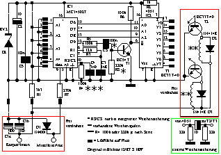 The adjacent circuit diagram is provided to give the general idea; further in this article you can find how to download the circuit diagram in legible size. The red marked areas on the diagram show those components not mounted on the board; they are free wired (soldered) into the track-body. The green framed section of the circuit describes an additional alternative protection of the turnouts and the decoder from the danger of coil burnout from a missing digital "off"-command.
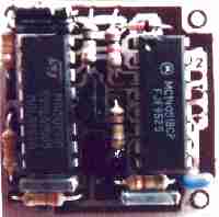
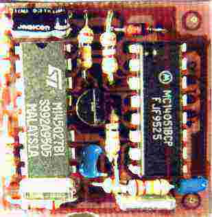
  I have replaced both Darlington-driver arrays with two BC337-40 with protection-diodes, because the arrays need too much space and for normal turnouts only two transistors are needed, and moreover these can be mounted at the turnouts coils . The base resistor for the driver transistors, R2 has been reduced to 1k. Furthermore I have soldered into the track-body a part of the voltage supply, namely the capacitor C1, as well as the rectifier-diode D1; moreover for space reasons I have split C1 into two capacitor (C1a and C1b) of 100µ each. The actual dimensions of the pcb artwork is 3.1 cm at the outer edges of the leader-tracks on each side.
  . Next comes the optional components CS and RS inserted at the input to T1. Note that for turnouts operation, the 4051 gets a control signal for between 150 and 300 ms so consequently the turnouts coil winding only has voltage applied for this time duration, so that if the "off"-command (all data-bits are "0") fails to arrive, or is not recognised, overheating and failure of T2/T3 or the coils will not occur. But if you wish to use the decoder partially for turnouts and partially for switching other circuits you may want to put in CS and RS, shown in the green framed circuit, before each driver-transistor - T2/ T3 - to provide a limit on the time duration of the output of the decoder. You find the layouts for it´s pcb at left side. You can download the layout in a bigger scale including the assembly-layout; the security-pcb´s scale is 2:1.
 The adjacent photograph shows the mounting into a standard M-turnout. Notice the placing of C1a / C1b and D1 as well as both driver-transistors and protection-diodes. The soldering to the track-body and supply rails necessitates a fairly powerful soldering iron; and the metal should be first thoroughly cleaned of any paint or dirt. The correct polarisations of the capacitors and the diodes is very important. At the coils of the turnouts-mechanism you must desolder the blue cables and also the yellow illumination-cables; the short yellow supply-connection for the lamp is connected to the supply voltage. This causes the lamp to burn without flickering; however if the lamp is too bright, especially at supply voltages of more than 16 V, you can put an appropriate zener diode in series, with the anode to the supply lead, and this will prevent the lamp from burning out too quickly. If you only have a small Booster and want to save all its energy for the
rolling stock, either abstain from using the illumination or use a seperate supply or use a big enough series zener to make the lamps only dim.
The adjacent photograph shows the mounting into a standard M-turnout. Notice the placing of C1a / C1b and D1 as well as both driver-transistors and protection-diodes. The soldering to the track-body and supply rails necessitates a fairly powerful soldering iron; and the metal should be first thoroughly cleaned of any paint or dirt. The correct polarisations of the capacitors and the diodes is very important. At the coils of the turnouts-mechanism you must desolder the blue cables and also the yellow illumination-cables; the short yellow supply-connection for the lamp is connected to the supply voltage. This causes the lamp to burn without flickering; however if the lamp is too bright, especially at supply voltages of more than 16 V, you can put an appropriate zener diode in series, with the anode to the supply lead, and this will prevent the lamp from burning out too quickly. If you only have a small Booster and want to save all its energy for the
rolling stock, either abstain from using the illumination or use a seperate supply or use a big enough series zener to make the lamps only dim.
The components:
For space-reasons only 1/4-Watt resistors should be used. For R2, R4, R5 and RS even 1/10-Watt resistors are recommended, because then the board can be installed at least 1 mm deeper. The capacitors are not allowed to be higher than 5 mm - and are better if lower. Same is valid for T1. If necessary the plastic body must be trimmed or you must use a similar transisor. CS should be only 2 or 3 mm high, otherwise there will not be enough space. A ceramics capacitor is very suitable for C5; naturally one could use also a SMD-capacitor. The diameter of C1a and C1b can not be bigger than 7 mm. The diameter of C2 should be less than 5 mm. Once completed, if the decoder doesn’t work despite correct code setting, and there are no construction mistakes, the time-constant may need changing. Using MC145027 until middle 1988 the values of R3=12k and R4=100k are correct. Using newer chips the values must be increased to R3=27k/22k and R4=220k. Sometimes combinations of 22k/100k are also working properly. Of course you also can modify the values of the caps.
Here is the parts list for the decoder itself without the security-circuit:
| R1 = 3k3 | C1a, C1b = 100 µ/25 V | D1 = 1N4001 |
| R2 = 1k | C2 = 10 µ/10 V radial | D2 = Z-Diode 8,2 V/400 mW |
| R3 = 12 k (27k) | C3 = 1n8/RM 7,5 | D3, D4 = 1N4148 |
| R4 - R6 = 100 k (R4=220k) | C4 = 3n9/RM 7,5 | T1 = BC 547 |
| R7 = 270 k | C5, CS = 100 n | T2, T3 = BC 337-40 |
| RS = 220 k | IC1 = MC145027 | |
| IC2 = CMOS 4051 |
The size of the components used is very important, to allow for the mounting into the turnouts. It is wise therefore to measure them before purchase. Procurement problems may occur for the MC145027, because these Motorola-chips are not the most current of semiconductors and are not that widely used for other purposes. If you can’t get them from your local Motorola dealer, one possible source is hobbycenter@hobbycenter.se.
Brave people who can not get to the parts or make the pcbs themself, can connect me; maybe I can help.
 The optional RSs and CSs are not taken into account in the board-layout; they can be added however quite easily. For this R5s end wire is soldered in only at the T1 end. At the other hole that is normally R5, CSs wire is soldered in; the free connection-wires of R5 and CSs are
connected together. At this connection RSs are also soldered, lying over R4 and with its other connection either in the free hole between R4 and C5 or soldered at C4. When using 1/4-Watt-types for R4 and RS it is recommended to solder R4 at the edge of the board parallel to C4 and RS at position of R4 in the mentionded free hole at C5. The left photograph shows the components in the first variation.
The optional RSs and CSs are not taken into account in the board-layout; they can be added however quite easily. For this R5s end wire is soldered in only at the T1 end. At the other hole that is normally R5, CSs wire is soldered in; the free connection-wires of R5 and CSs are
connected together. At this connection RSs are also soldered, lying over R4 and with its other connection either in the free hole between R4 and C5 or soldered at C4. When using 1/4-Watt-types for R4 and RS it is recommended to solder R4 at the edge of the board parallel to C4 and RS at position of R4 in the mentionded free hole at C5. The left photograph shows the components in the first variation.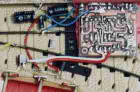 The protection-diodes D3 and D4 are soldered between the coil connection. T2 and T3 are soldered with their collector leads at the outer coil connections; the emitters soldered together and with a scrap of wire to ground, i.e. the connection of D1 with C1a/ C1b. The right photograph - a cutout out of the foregoing illustrates this and shows the wiring. If you want to provide each coil with its own pulse duration protection instead of RSs and Css, solder in the components shown in the green marked circuit diagram at the input to each driver-transistor; pay attention to the correct polarisation (the minus-pole goes to the base of T2 or T3); the opposite lead to ground ie the emitter lead of the transistors.
For space reasons the setting the code is done with solder links, not through switches. Each of the four address-inputs of the MC145027 are connected to ground, or supply, or left open. Be careful that no pin is connected to both supply and ground together! The function of these connections is the same as the settings of the 8 pole DIL switch on the loco-Digital-Decoder; also the designation of the solder bridge in the circuit diagram is identical with this. Setting the codes is listet in the table and follows therefore the corresponding explanation in the service-instructions for Digital- and Delta-locomotives; for example, the address of 0 for all inputs open. In the Elektor German-issue 7/ 78, p.21, is a table printed, relating to the use of the Märklin-keyboard; in German-issue 4/ 89 p. has printed a table for achieving 81
addresses. Carsten Meyer provides a similiar explanation in German. And finally you can calculate the adress with the formlua
dekoderadress = key-no. + (16 * (keyboardno. -1)).
For example: If you want to adress the 8. key aof the 4. keyboard the formula looks like:
dekoderadress = 8 + (16 * (4 - 1) = 56. When using the IntelliBox you must add "3" to the adress, because we can use the main-adress 0 wiht our decoder, which is used by Märklin and Uhlenbrock only in the idle-mode. This means that the IB-adress 56 must be adjusted at the decoder as adress 59 according to our adress-table. Vice versa you can switch a turnout with the adress 59 according our table when adjusting the IB to it´s adress 56.
If one uses however a different control for example a self-built controller or a software-controller, one can control more then 256 turnouts or 512 magnet items. Because the four ternary address-bits can adress 81 decoder-addresses and each decoder has 8 sub-addresses (switch connections), that can be addressed through the binary data-bits of the pulse, one can control up to 324 turnouts or 648 magnet items. This should suffice for even the biggest of layouts. However if this is still is not enough, one can also connect A5 of the MC145027 to the plus supply and consequently control further 324 turnouts or 648 magnet items; however the controller must have the ability to send out pulses with bit 5 set; this is the manner used by the function-decoders in controlling for example the dance and panorama-cars.
The preceding explanations and photographs refer to the usual power supply of decoders from the negative track voltage. The ground of the decoder is connected to the negative track voltage, which has a significant drawback: Since the data signals are asymmetrically shifted to the negative voltage it has to cope an additional load during the activation of a turnout. Under heavy duty operation and/or a low- powered booster this can lead to a collapse of the negative track voltage and thus to distinct drop-outs of running locos during turnout activation. This can be avoided by operating the decoder on the positive voltage: the ground of the decoder is then linked with the ground of the booster. The connection is to be made according to the marked (****) sections in the wiring diagram; D1 has to be reversed then. Of course in this case the assembly instructions mentioned above do not apply.
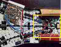
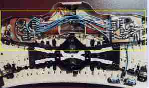
 The mounting of the decoder into the three way turnout is shown in the two adjacent pictures. At right is a cutout-enlargement showing the wiring of the coils. You can see the network of diodes which is described below.
The peculiarity of the three way turnout is, that they have two coil bodies and therefore four coils. The two mechanisms are independent, necessitating that for switching from "on the left" to "on the right" two switching processes: Of "on the left" to "straight-out of" with the left coils and of "straight-out of" to "on the right" with the coils on the right.
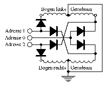 The connection at the turnouts-decoder offers the possibility, to combine this twofold switch event into one command. For this purpose only three transistor outputs are used. The four transistors - two for each double coil - are switched together and connected to the three decoder-outputs via diodes in the base-connections, so that the first output switches both coils to "straight-out of," the next output the left coil to "on the left" as well as the right coil to "straight-out of" and finally the third output the left coil on "straight-out of" as well as the right coil to "on the right". The adjacent sketch - which to give a better view has the transistors and protection-diodes missing - makes this plain. Maybe you can use the mechanical synchronisation from Märklin-Magazin issue 2/75 p.16 (in German) and therefore switch with the first output both coils to "straight-out of," with the next output only the left coil to "on the left" and finally with the third output only the right coil to "on
the right". This may work but I have not tested it.
The connection at the turnouts-decoder offers the possibility, to combine this twofold switch event into one command. For this purpose only three transistor outputs are used. The four transistors - two for each double coil - are switched together and connected to the three decoder-outputs via diodes in the base-connections, so that the first output switches both coils to "straight-out of," the next output the left coil to "on the left" as well as the right coil to "straight-out of" and finally the third output the left coil on "straight-out of" as well as the right coil to "on the right". The adjacent sketch - which to give a better view has the transistors and protection-diodes missing - makes this plain. Maybe you can use the mechanical synchronisation from Märklin-Magazin issue 2/75 p.16 (in German) and therefore switch with the first output both coils to "straight-out of," with the next output only the left coil to "on the left" and finally with the third output only the right coil to "on
the right". This may work but I have not tested it.
 Although the double-crossing-turnouts require more space for the decoding than the standard turnouts, in fact they have less overall interior space, so that the normal board does not fit in. So for these units I have apportioned the circuit between two littler boards. One can do it similar, built a special
SMD-decoder or wait until the C-turnout-decoder is available and try to make it fitting into the
crossing-turnout.
Although the double-crossing-turnouts require more space for the decoding than the standard turnouts, in fact they have less overall interior space, so that the normal board does not fit in. So for these units I have apportioned the circuit between two littler boards. One can do it similar, built a special
SMD-decoder or wait until the C-turnout-decoder is available and try to make it fitting into the
crossing-turnout.
